Production
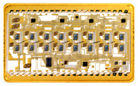
Thinfilm Hybrids
Substrate Materials:
- ceramics Al2O3, AlN
- Glass, Quartz and Fused Silica, Sapphire
- Si, SiC, others on request
Layer Systems:
- different CrNi/Au-systems , e.g. CrNi/W/Ti/Pd/Au
- Cu based systems
- other layer compositions on request
Resistors:
- CrNi-substrate resistors (integrated) with surface resistivities from 10?/? to 300?/?
- <25ppm/K, trim to 0.01%
- chip resistors (dice) from 0.1?-100G?
- standard resistors (glued or soldered)
Suitable for:
- soldering techniques
- gluing techniques
- bonding (Al and Au)

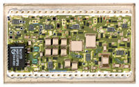
Thickfilm Hybrids
Substrate Materials:
- ceramics Al2O3 (4in x 4in)
- ceramics AlN (2in x 2in)
- others on request
Conductors:
- PdAg, Au, Ag, PtAg
- min. 80µm (3.15mil) distance, min. 100µm (4mil) width
Resistors:
- thickfilm resistors (integrated), trim down to 0.1%
- <25ppm/K, trim to 0.01%
- chip resistors (dice) from 0.1? - 100G?
- standard resistors (glued or soldered)
Suitable for:
- soldering techniques
- gluing techniques
- bonding (Al and Au)

Chip on Board (COB)
COB technology on PCB and Flex materials. Other base materials on request.
Assembly
Assembly - Placement:
- all standard components
- dice, unpackaged components/semiconductors
- precision mounting of optical components (CCD, LED, sensor etc.)
Assembly of Modules and Appliances:
- assembly of modules and appliances by commissioned production
- manufacturing and test of optical modules and appliances
Documentation
Documentation and security rules are enforced on a high level:
- 100% traceability
- detailed test documentation
Packaging
Packaging:
- Packaging of Hybrids and Printed Circuit Boards
- Packages for special applications
- MEMS-Packaging
- Packaging of optical components


